1~2 Cell Dry Battery Powered Ultra Low Quiescent Current Synchronous Boost DC-DC Voltage Regulator IC OC6813
Popular Search Keywords: low quiescent current boost IC, synchronous boost DC-DC, 1.5V to 3.3V boost converter, dry cell boost IC, SOT23-3 boost chip, OC6813 distributor, OC6813 datasheet, low power boost regulator, 15uA standby current, blood pressure monitor boost IC, wireless keyboard power IC, electronic dictionary power supply
OC6813 Key Features: Standby current only 15uA (Typical 6uA quiescent current) | Ultra low startup voltage down to 0.9V | Peak efficiency up to 93% | Constant On-Time PFM Control | Auto frequency reduction at light load | Only 3 external components required | Output voltage customizable from 2.2V~5.0V | Dual package: SOT23-3 / SOT23-5
Keywords: OC6813, OC6813T25, OC6813T33, OC6813L33, OC6813T36, OC6813L36, ultra low quiescent current synchronous boost DC-DC, dry cell boost IC, 1.2V to 3.3V boost converter, low power boost regulator, SOT23-3 boost converter, portable device power IC, blood pressure monitor power solution, wireless keyboard boost IC, electronic dictionary DC-DC, toy power boost chip
Product Description: OC6813 series are ultra low quiescent current synchronous boost DC-DC converters launched by OCX, specifically designed for portable devices powered by 1~2 cell dry batteries. The typical standby input current is only 15uA. It adopts PFM control to automatically reduce switching frequency under light load, maintaining high efficiency across full load range. The ultra low startup voltage of 0.9V maximizes battery energy utilization. This IC only requires one inductor, one input capacitor and one output capacitor for normal operation. The output voltage can be customized from 2.2V to 5.0V with 0.1V step. It is available in SOT23-3 (without EN pin) and SOT23-5 (with EN enable pin) packages, widely used in electronic dictionaries, digital cameras, blood pressure monitors, MP3 players, wireless mouse & keyboard, medical devices, anti-lost trackers, vehicle anti-theft devices and other portable handheld products.
OC6813 Ordering Information & Package Selection
OC6813 Ordering Table / Output Voltage & Package Options
| Part Number | Output Voltage | Package | Enable Pin (EN) |
| OC6813T25 | 2.5V | SOT23-3 | No |
| OC6813T33 | 3.3V | SOT23-3 | No |
| OC6813L33 | 3.3V | SOT23-5 | Yes |
| OC6813T36 | 3.6V | SOT23-3 | No |
| OC6813L36 | 3.6V | SOT23-5 | Yes |
| Custom Voltage | 2.2V~5.0V
(0.1V Step) | SOT23-3 / SOT23-5 | Optional |
※ Standard Packaging: 3000 pcs / reel. Please contact our sales team for customized output voltage.
OC6813 Core Advantages
● Ultra low standby current: Typical 15uA input current (6uA quiescent current), greatly extend battery life
● Ultra low startup voltage at 0.9V, compatible with single dry battery operation
● Synchronous rectifier architecture, peak efficiency up to 93%, no external Schottky diode required
● PFM control mode with auto frequency reduction at light load, high efficiency over full load range
● Minimal external components: Only inductor, input capacitor and output capacitor (3 components total)
● Flexible output voltage: Customizable from 2.2V to 5.0V with 0.1V step
● Low ripple & low noise, ideal for sensitive analog circuit power supply
● Built-in over-current protection & thermal shutdown protection for high reliability
OC6813 Key Electrical Parameters
| Parameter | Typical Value | Unit |
| Input Voltage Range | 0.9 ~ 5.0 | V |
| Startup Voltage | 0.9 | V |
| Output Voltage Range | 2.2 ~ 5.0 (0.1V Step) | V |
| Quiescent Current (No Load) | 6 | μA |
| Standby Input Current (VIN=1.2V, VOUT=3.3V) | 15 | μA |
| Maximum Switching Frequency | 370 | kHz |
| Efficiency (VIN=1.2V, VOUT=3.3V, IOUT=10mA) | 88 | % |
| Peak Efficiency | 93 | % |
| Output Ripple | Typical 30 | mV |
OC6813 Pinout Definition
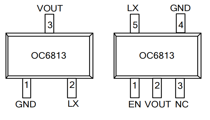
| SOT23-3 Pin No. | SOT23-5 Pin No. | Pin Name | Function Description |
|---|
| 1 | 4 | GND | Ground |
| 2 | 5 | LX | Switch Node, Connect to Inductor |
| 3 | 2 | VOUT | Output Voltage Feedback / Output Terminal |
| - | 1 | EN | Chip Enable Control, Active High |
| - | 3 | NC | No Connection |
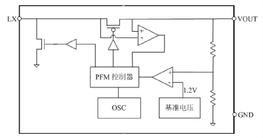
OC6813 Internal Block Diagram
OC6813 Typical Application Circuit
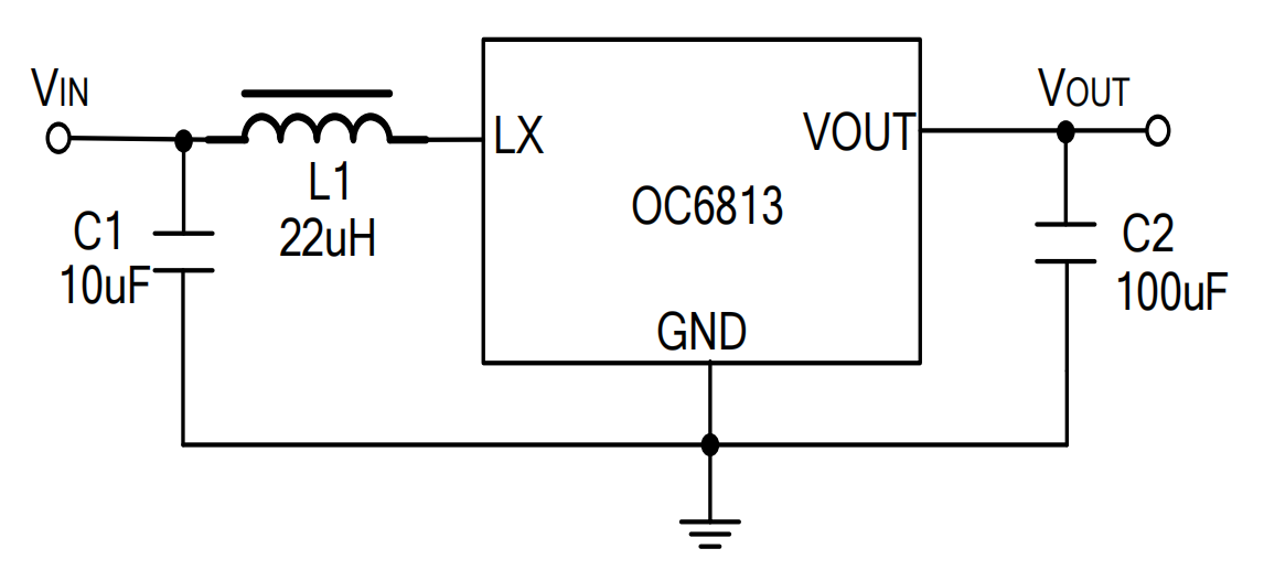
※ Typical Application: L=22μH~47μH, CIN=10μF, COUT=22μF (Ceramic Capacitor). Pull EN pin high to enable the IC, pull low to disable.
OC6813 Absolute Maximum Ratings
Absolute Maximum Ratings (Note 1)| Symbol | Description | Rating | Unit |
|---|
| VMAX | Maximum Voltage on LX, VOUT Pins | 5 | V |
| PSOT | Maximum Power Dissipation (SOT23 Package) | 0.2 | W |
| TA | Operating Ambient Temperature Range | -20~85 | ℃ |
| TSTG | Storage Temperature Range | -40~120 | ℃ |
| TSD | Soldering Temperature (Duration < 30s) | 240 | ℃ |
| VESD | ESD Withstand Voltage (Human Body Model) | 2000 | V |
Note: Exceeding the listed absolute maximum ratings may cause permanent damage to the device. Operation under absolute maximum conditions may affect device reliability.
OC6813 Electrical Characteristics
| Electrical Parameters | Symbol | Test Conditions | Min | Typ | Max | Unit |
|---|
| Output Voltage Accuracy | Δ VOUT |
| -2.5 |
| 2.5 | % |
| Startup Voltage | VSTART | ILOAD=1mA, VIN:0→2V |
| 0.9 |
| V |
| Hold Voltage | VHOLD | ILOAD=1mA, VIN:2→0V | 0.6 |
|
| V |
| Conversion Efficiency | η |
|
| 93 |
| % |
| No-Load Input Current | IIN | VIN=1.5V, VOUT=3.3V |
| 15 |
| uA |
| Quiescent Current | IS | VOUT=VOUT_TAR+0.5V |
| 6 |
| uA |
| Maximum Duty Cycle | DUTY |
|
| 80 |
| % |
| Maximum Switching Frequency | Fmax |
|
| 370 |
| KHz |
OC6813 Application Fields
● 1~2 Cell Dry Battery / Ni-MH Battery Powered Devices (Electronic Dictionary, Digital Camera, Blood Pressure Monitor, MP3 Player)
● Wireless Mouse & Keyboard, Remote Control Toys, Wireless Headphones
● Medical Devices (Blood Glucose Meter, Thermometer, Anti-Lost Tracker)
● Vehicle Anti-Theft Device, Charger, VCR, PDA and other handheld devices
● Low Power IoT Sensor Nodes, Portable Meters
● Any application requiring low voltage battery boost to 3.3V/5V with long standby time
OCX Low Power Boost Converter Series Recommendation
| Part Number | Input Voltage | Output Voltage | Output Current | Quiescent Current | Package | Features |
| OC6813 | 0.9~5V | 2.2~5V | Max 200mA | 6μA | SOT23-3/5 | 15μA ultra low standby current, minimal external components |
| OC6800 | 0.8~3.3V
| Fixed 3.3V | 150mA | 10μA | SOT23-3 | Ultra low startup voltage, ideal for single cell battery |
| OC6815 | 0.9~5V | Adjustable / Fixed | 500mA | 30μA | SOT23-6 | High output current, with output disconnect function |
※ Please contact our technical team for more models and customized output voltage.
OC6813 Drop-in Replacement & Compatibility Guide
OC6813 is pin-to-pin compatible with the following models (Please verify voltage and package): TPS61098, ME2108, MT3608(Partial), BL8530, XC9103 and other low power boost ICs. Compared with similar products, OC6813 features lower standby current (15uA vs 30uA+), lower startup voltage (0.9V) and fewer external components.
Authorized Distributor & Service
GS Micro Semiconductor (Shenzhen) Co., Ltd. is an authorized first-tier distributor of OCX, focusing on power management and low power IC solutions. We supply full range of OCX boost DC-DC products including OC6813, OC6800 and OC6815, providing high-reliability & long standby power solutions for portable devices, medical electronics and IoT applications. We have warehouses in Shenzhen, Shanghai and Beijing, supporting fast delivery across China and overseas.